Marketing Chen
Marketing Cai
Recently Prof. Chun Li and Associate Prof. Changyong Lan of the University of Electronic Science and Technology (UEST) have worked on a differential pressure sensor based on a non-transferring piezoresistive PdSe2 polycrystalline film. In this study, a differential pressure sensor based on non-transferring piezoresistive PdSe2 polycrystalline film was prepared based on the change of resistance under the action of film flexure and finite element strain analysis. This transfer-free and low-temperature-grown PdSe2 piezoresistive film has promising applications in MEMS sensor devices. The study was published under the title "Differential pressure sensors based on transfer-free piezoresistive layered PdSe2 thin films" in the journal Nanotechnology.
The two professors used the silicon nitride film independently developed and produced by YW MEMS (Suzhou) Co., Ltd. as the carrier in their research, and patterned the Pd coating on the flat and clean silicon nitride film by magnetron sputtering. It was found that the strain coefficients of the PdSe2 film, which was prepared by the PES predeposition method, were superior to that of the polycrystalline silicon film. Upon investigation, it was found that the excellent piezoresistive properties, pressure sensitivity, and CMOS process synthesis method of PdSe2 thin films offer a lot of potential for the integration of MEMS sensors.
The original text follows:
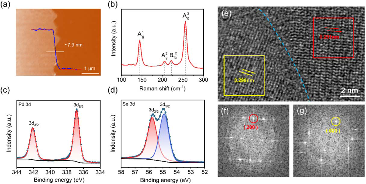
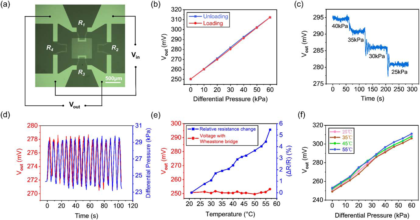
In this study, the authors obtained transfer-free piezoresistive PdSe2 polycrystalline films by direct sputtering of Pd on SiNx films and plasma-enhanced selenization of Pd metal films at temperatures as low as 200°C. The films were characterized by a high strain coefficient (GF) of - 43.3. Based on the resistance change under film flexure and finite element strain analysis, the strain factor (GF) of 7.9 nm thick PdSe2 film was found to be - 43.3, which is better than that of polycrystalline silicon film (GF 8~20). The large GF enables the diaphragm pressure sensor to have a higher sensitivity of 3.9 × 10⁻⁴ kPa-1 in the differential pressure range of 0 - 60 kPa. In addition, the sensor with a Wheatstone bridge circuit achieves a high voltage sensitivity of 1.04 mV-kPa-1 and a fast response time of less than 97 ms.

Characterization of PdSe2 thin films. (a) Surface morphology of the PdSe2 thin film obtained by AFM, the corresponding height distribution map shows that the thickness of the prepared PdSe2 is 7.9 nm.(b) Raman spectra of the prepared PdSe2 thin film. (c), (d) XPS peaks of Pd 3d and Se 3d. (e) HRTEM images of PdSe2 polycrystalline films. (f) and (g) FFT corresponding to the red and blue regions in (e), respectively.

Performance of a PdSe2 differential pressure sensor using a Wheatstone bridge circuit. (a) Photograph of the PdSe2 differential pressure sensor unit connected in the Wheatstone bridge circuit. (b) Output voltage of the sensor in the range of 0 - 60 kPa during loading (pressurization) and unloading (depressurization). (c)Output voltage of the device when there is a step change in differential pressure (25 - 40 kPa). (d) Output voltage profile when there is a small perturbation change in the differential pressure. (e) Variation of relative resistance of PdSe2 resistor with increasing temperature (blue curve) and output voltage of the device under Wheatstone bridge versus increasing temperature (red curve). (f) Curves of differential pressure versus output voltage for differential pressure sensors at different temperatures.

In this study, a highly sensitive differential pressure sensor based on a PdSe2 polycrystalline thin film was fabricated and the feasibility of a two-dimensional semiconductor thin film for use in MEMS differential pressure sensors was demonstrated. The sensor has excellent differential pressure tracking performance even under small differential pressure oscillations. Transfer-free and low-temperature PES ensures the efficiency and success of device preparation. It can be used for barometric pressure monitoring, ventilation system pressure control, blood pressure monitoring, and other applications where the pressure is lower than 100 kPa. The authors concluded that the excellent piezoresistive properties, pressure sensitivity, and CMOS process synthesis method of PdSe2 thin films offer many potentials for MEMS sensor integration.
This research was supported by the National Natural Science Foundation of China, the Natural Science Foundation of Sichuan Province, and the Sichuan Science and Technology Program.
YW MEMS (Suzhou) Co., Ltd) silicon nitride film was used as the carrier, and Pd-patterned Pd coating was applied on the flat and clean silicon nitride film by magnetron sputtering, and PdSe2 polycrystalline ultrathin films were prepared by PES pre-deposition method, which enabled the experiments to be carried out smoothly.